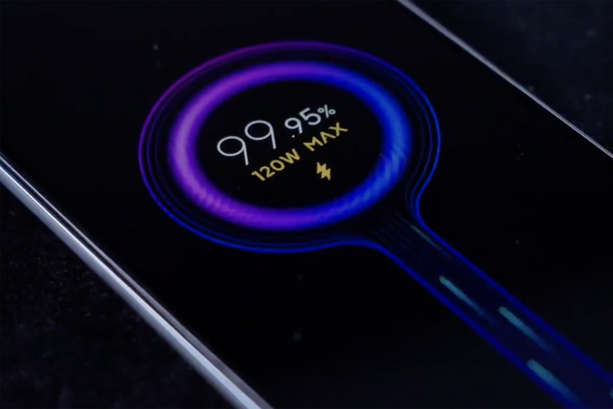
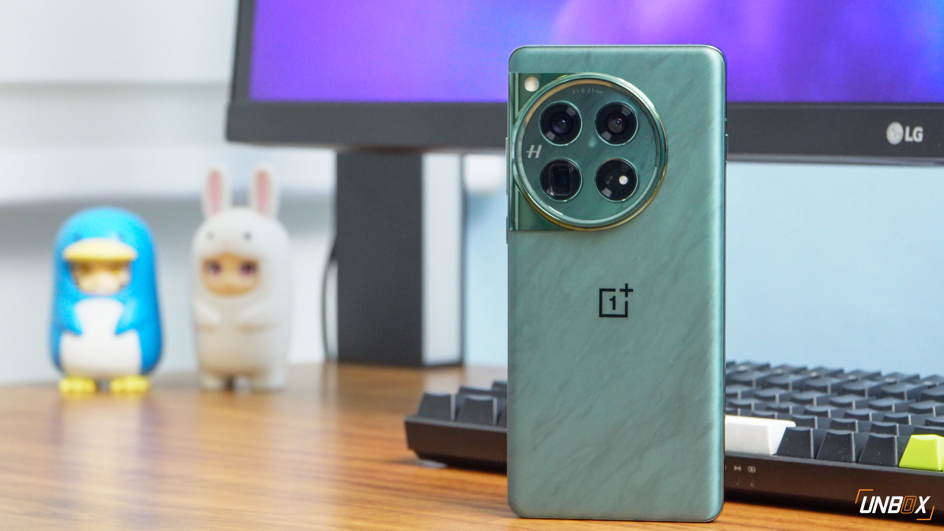
The smartphone battery life war is going on as we speak. Manufacturers are racing to see who can cram the biggest battery in their devices without sacrificing ergonomics or aesthetics. Charging speeds also seem to be a contending point, with companies like Xiaomi and Qualcomm trying to reach the coveted 200W mark. For reference, first-generation fast chargers had a wattage of around 18. Now, in addition to these specifications and the improvement of smartphone thermals, chipmakers like Samsung and IBM are looking to take things much further in order to promise extended week-long battery life through chipset development, according to a report by Gizmodo. All this research seeks to make smartphone processors more efficient with power management without sacrificing capability.
This technology-in-development is called vertical transport field-effect transistors (VTFETs), which from a technical perspective should be 85% more power-efficient than the current-day fin field-effect transistors (FinFETs).

Graph courtesy of evobsession.
How does it achieve such a feat? To put it simply, scientist Gordon Moore came up with Moore’s Law in 1965. This states that the number of transistors you could place on a microchip double every 2 years due to the progression of technology, the cost of CPUs, and the size of a transistor relative to performance. If you can cram more of the same smaller transistors onto the same board, then you receive improved computing performance in return.
Current processor technologies indicate that we’re reaching the limits of how tiny we can make the transistor, with 4 nanometers being our smallest as of now. While our flagship chipsets are by no means as thirsty as years ago, there is still some way to go. As we rapidly close out towards 1 nanometer as the limit of what technology can achieve as of the moment, companies are now changing their approach – tinkering not only with the size of the transistors but how the layout can be changed to improve efficiency.
Smartphone chipset boards as of the moment are just a flat 2D space, with transistors next to each other. Samsung, IBM Intel, and other companies understand that battery life is important for consumers, as these people prefer not to worry about their devices turning to paperweight while they’re on the go. To this end, they’ve continued innovating on the vertical plane – stacking transistors in order to increase transistor density and improve power current flow (from horizontal to vertical). Should they succeed, we could be seeing much longer battery life on our consumer devices than we are now. However, there’s no strict timeline on when this technology will be made available to the public and if it is even financially feasible enough for mass production. We’ll just have to wait and see.


